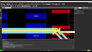
Media Summary: Easily meet length and phase pin-to-pin constraints as traces bend without creating electrical issues. Get the FREE Have you ever tried to use the relative propagation delay pin group option for length matching rather than matching through the ... Cadence Allegro PCB Differential Pair Routing

Dynamic Differential Pair Routing Orcad Pcb Designer - Detailed Analysis & Overview

Easily meet length and phase pin-to-pin constraints as traces bend without creating electrical issues. Get the FREE Have you ever tried to use the relative propagation delay pin group option for length matching rather than matching through the ... Cadence Allegro PCB Differential Pair Routing 透過動態的差動相位控制,可以同步驗證差動對的長度匹配並符合其相位約束規則,而不會產生電氣問題。 使用 I come up with this a long time ago and keep using it all the time. Links: - To learn how to Electrons don't just travel from just pin to pin on single layers. They can travel in the z-axis through vias and pins as well as inside ...

In this video, we'll walk you through the process of assigning

Photo Gallery

Dynamic Differential Pair Routing | OrCAD PCB Designer
Cadence Differential Pair Dynamic Phase
How to use Dynamic Differential Pair Routing in OrCAD Real-Time PCB Design
Cadence PCB Diff Pair Physical Rules Routing
How to create Differential pair signals in the Constraint Manager using the OrCADX Capture Schematic
Relative propagation delay for length matching traces OrCAD
Cadence OrCAD PCB Design How to Set Trace Impedance (Signal Integrity)
Cadence Allegro PCB   Differential Pair Routing
How To Constrain Differential Pairs in OrCAD X
Dynamic Neck-Down Tapers for Differential Pairs Using The Teardrops and Trace Drops Forms
Tutorial Differential Pair OrCAD Allegro
動態差動對走線 (Differential Pair)-【即時高速訊號設計】
View Detailed Profile
Dynamic Differential Pair Routing | OrCAD PCB Designer

Dynamic Differential Pair Routing | OrCAD PCB Designer

Differential

Cadence Differential Pair Dynamic Phase

Cadence Differential Pair Dynamic Phase

Here we explore the

How to use Dynamic Differential Pair Routing in OrCAD Real-Time PCB Design

How to use Dynamic Differential Pair Routing in OrCAD Real-Time PCB Design

Easily meet length and phase pin-to-pin constraints as traces bend without creating electrical issues. Get the FREE

Cadence PCB Diff Pair Physical Rules Routing

Cadence PCB Diff Pair Physical Rules Routing

Here we explore the

How to create Differential pair signals in the Constraint Manager using the OrCADX Capture Schematic

How to create Differential pair signals in the Constraint Manager using the OrCADX Capture Schematic

OrCAD

Relative propagation delay for length matching traces OrCAD

Relative propagation delay for length matching traces OrCAD

Have you ever tried to use the relative propagation delay pin group option for length matching rather than matching through the ...

Cadence OrCAD PCB Design How to Set Trace Impedance (Signal Integrity)

Cadence OrCAD PCB Design How to Set Trace Impedance (Signal Integrity)

NEW Methodical Method to Hardware &

Cadence Allegro PCB   Differential Pair Routing

Cadence Allegro PCB Differential Pair Routing

Cadence Allegro PCB Differential Pair Routing

How To Constrain Differential Pairs in OrCAD X

How To Constrain Differential Pairs in OrCAD X

Signal

Dynamic Neck-Down Tapers for Differential Pairs Using The Teardrops and Trace Drops Forms

Dynamic Neck-Down Tapers for Differential Pairs Using The Teardrops and Trace Drops Forms

Xpedition Package

Tutorial Differential Pair OrCAD Allegro

Tutorial Differential Pair OrCAD Allegro

Here we explore the

動態差動對走線 (Differential Pair)-【即時高速訊號設計】

動態差動對走線 (Differential Pair)-【即時高速訊號設計】

透過動態的差動相位控制,可以同步驗證差動對的長度匹配並符合其相位約束規則,而不會產生電氣問題。 使用

Differential Pair Setup and Routing Matching Techniques in PCB Design #68

Differential Pair Setup and Routing Matching Techniques in PCB Design #68

Welcome to our comprehensive KiCad

Useful TIP: What Track Width To Use When Routing PCB?

Useful TIP: What Track Width To Use When Routing PCB?

I come up with this a long time ago and keep using it all the time. Links: - To learn how to

(Sponsored) Differential Pairs - PCB Design Basics - Phil's Lab #83

(Sponsored) Differential Pairs - PCB Design Basics - Phil's Lab #83

Differential pair PCB design

High-Speed Signal Routing : Z-Axis and Package Pin Delay | OrCAD PCB Designer

High-Speed Signal Routing : Z-Axis and Package Pin Delay | OrCAD PCB Designer

Electrons don't just travel from just pin to pin on single layers. They can travel in the z-axis through vias and pins as well as inside ...

Differential Pair Phase Matching

Differential Pair Phase Matching

See how HyperLynx DRC's

Cadence PCB Delay Tune

Cadence PCB Delay Tune

Here we explore the

How to Define Differential Pairs in OrCAD Capture 17.2

How to Define Differential Pairs in OrCAD Capture 17.2

Capture

OrCAD How-To -Creating Differential Pairs Tutorial Cadence Allegro

OrCAD How-To -Creating Differential Pairs Tutorial Cadence Allegro

In this video, we'll walk you through the process of assigning