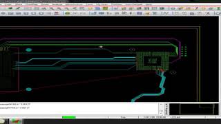
Media Summary: Cadence PCB Editor Timing Vision Tutorial Cadence PCB Editor Suites 2 Minute Overview OrCAD and Allegro When routing a bus or a group of specific signals, you need to maintain similar etch length for all the signals in the group.
Cadence Pcb Delay Tune - Detailed Analysis & Overview
Cadence PCB Editor Timing Vision Tutorial Cadence PCB Editor Suites 2 Minute Overview OrCAD and Allegro When routing a bus or a group of specific signals, you need to maintain similar etch length for all the signals in the group. Have you ever tried to use the relative propagation Cadence Allegro Timing Vision Environment1 In Altium Designer 20.0, you can now selectively monitor propagation
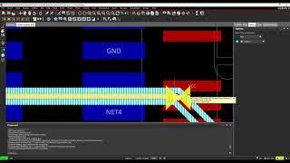
Electrons don't just travel from just pin to pin on single layers. They can travel in the z-axis through vias and pins as well as inside ...