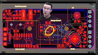
Media Summary: I come up with this a long time ago and keep using it all the time. Links: - To learn how to design boards have a look at FEDEVEL ... Grab your free Design Mistakes Checklist Bundle: ... I challenged a software engineer to design his very first

Quick Tips Pcb 30 Set Traces To Follow Components In Pcb - Detailed Analysis & Overview

I come up with this a long time ago and keep using it all the time. Links: - To learn how to design boards have a look at FEDEVEL ... Grab your free Design Mistakes Checklist Bundle: ... I challenged a software engineer to design his very first This video is made possible by PCBWay. Submit your tutorial here: ... We will start a series of videos from scratch on learning to design KiCad Layout: Vias and Footprint Changes (Part 7)

Photo Gallery

Quick Tips [PCB 30]: Set Traces to Follow Components in PCB
Best Practices for PCB Part Placement (Part 1)
(Sponsored) PCB Traces 101 - Phil's Lab #112
Component Selection Process Tips for PCB Design
EEVblog #1323 - PCB Layout Review & Analysis
Useful TIP: What Track Width To Use When Routing PCB?
Top 5 Beginner PCB Design Mistakes (and how to fix them)
6 Horribly Common PCB Design Mistakes
Do you also make these mistakes in PCB Layout?
Mastering PCB Part Placement: Plan the Perfect Layout with Flux
PCB Design For Beginners:  Ugly Tracks Are Noisy
My Top 10 PCB Design Tips
View Detailed Profile
Quick Tips [PCB 30]: Set Traces to Follow Components in PCB

Quick Tips [PCB 30]: Set Traces to Follow Components in PCB

This video is part of the EasyEDA

Best Practices for PCB Part Placement (Part 1)

Best Practices for PCB Part Placement (Part 1)

PCB

(Sponsored) PCB Traces 101 - Phil's Lab #112

(Sponsored) PCB Traces 101 - Phil's Lab #112

Basics and guidelines for

Component Selection Process Tips for PCB Design

Component Selection Process Tips for PCB Design

Altium Develop helps your team evaluate

EEVblog #1323 - PCB Layout Review & Analysis

EEVblog #1323 - PCB Layout Review & Analysis

Dave analyses a

Useful TIP: What Track Width To Use When Routing PCB?

Useful TIP: What Track Width To Use When Routing PCB?

I come up with this a long time ago and keep using it all the time. Links: - To learn how to design boards have a look at FEDEVEL ...

Top 5 Beginner PCB Design Mistakes (and how to fix them)

Top 5 Beginner PCB Design Mistakes (and how to fix them)

Altium Develop helps your

6 Horribly Common PCB Design Mistakes

6 Horribly Common PCB Design Mistakes

Grab your free Design Mistakes Checklist Bundle: ...

Do you also make these mistakes in PCB Layout?

Do you also make these mistakes in PCB Layout?

I challenged a software engineer to design his very first

Mastering PCB Part Placement: Plan the Perfect Layout with Flux

Mastering PCB Part Placement: Plan the Perfect Layout with Flux

Avoid the most common

PCB Design For Beginners:  Ugly Tracks Are Noisy

PCB Design For Beginners: Ugly Tracks Are Noisy

I laid out dozens and dozens of

My Top 10 PCB Design Tips

My Top 10 PCB Design Tips

This video is made possible by PCBWay. Submit your tutorial here: ...

How to clean up traces and vias in a PCB in KICAD #30

How to clean up traces and vias in a PCB in KICAD #30

We will start a series of videos from scratch on learning to design

KiCad Layout Vias and Board Modifications | Part 7 | PCB Design Tips

KiCad Layout Vias and Board Modifications | Part 7 | PCB Design Tips

KiCad Layout: Vias and Footprint Changes (Part 7) |