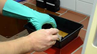
Media Summary: Josh talks about how we physically create electronic devices in the silicon wafers created in Part 1 of this series! To see the entire ... Support me on Patreon: In this video I attempt to use a laser printer and off-the-shelf PCB ... Peter Su, PhD student in the MIT Materials Science and Engineering program, explained the

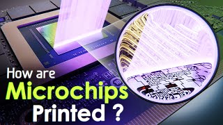
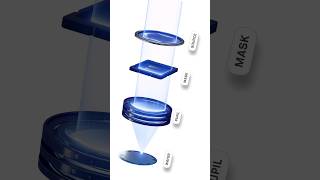
Photolithography Process For Planar Microwave Circuits - Detailed Analysis & Overview

Josh talks about how we physically create electronic devices in the silicon wafers created in Part 1 of this series! To see the entire ... Support me on Patreon: In this video I attempt to use a laser printer and off-the-shelf PCB ... Peter Su, PhD student in the MIT Materials Science and Engineering program, explained the Try SendCutSend 15% off for your next project! My descent into madness, chasing one ... In this video I demonstrate how I used a Carl Zeiss S- Interested in working on the forefront of technological innovation at ASML? Discover here: ...

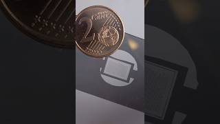
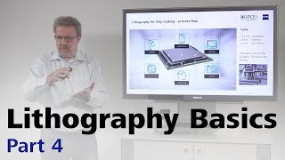
Bernd Geh The Key of Micro- and Nanoelectronics: Basics of Semi-conductive silicon wafer dicing,grinding and

Photo Gallery

Photolithography Process for Planar Microwave Circuits
Creating Circuits On A Silicon Wafer - How Sand Becomes Computers (2 of 6)
Photolithography on Silicon with PCB Chemicals
Photolithography: Step by step
‘Semiconductor Manufacturing Process’ Explained | 'All About Semiconductor' by Samsung Semiconductor
Photolithography
Photolithography tutorial
Speedrunning 30yrs of lithography technology
Photolithography #science #physics #experiment
DIY Photolithography using 1980s Carl Zeiss S-Planar Lens (405nm)
The $200M Machine that Prints Microchips:  The EUV Photolithography System
Extreme ultraviolet (EUV) Lithography Machine
View Detailed Profile
Photolithography Process for Planar Microwave Circuits

Photolithography Process for Planar Microwave Circuits

The video explains the fours

Creating Circuits On A Silicon Wafer - How Sand Becomes Computers (2 of 6)

Creating Circuits On A Silicon Wafer - How Sand Becomes Computers (2 of 6)

Josh talks about how we physically create electronic devices in the silicon wafers created in Part 1 of this series! To see the entire ...

Photolithography on Silicon with PCB Chemicals

Photolithography on Silicon with PCB Chemicals

Support me on Patreon: https://www.patreon.com/projectsinflight In this video I attempt to use a laser printer and off-the-shelf PCB ...

Photolithography: Step by step

Photolithography: Step by step

Photolithography: Step by step

‘Semiconductor Manufacturing Process’ Explained | 'All About Semiconductor' by Samsung Semiconductor

‘Semiconductor Manufacturing Process’ Explained | 'All About Semiconductor' by Samsung Semiconductor

What is the

Photolithography

Photolithography

How integrated

Photolithography tutorial

Photolithography tutorial

Peter Su, PhD student in the MIT Materials Science and Engineering program, explained the

Speedrunning 30yrs of lithography technology

Speedrunning 30yrs of lithography technology

Try SendCutSend 15% off for your next project! https://sendcutsend.com/breakingtaps/ My descent into madness, chasing one ...

Photolithography #science #physics #experiment

Photolithography #science #physics #experiment

Photolithography #science #physics #experiment

DIY Photolithography using 1980s Carl Zeiss S-Planar Lens (405nm)

DIY Photolithography using 1980s Carl Zeiss S-Planar Lens (405nm)

In this video I demonstrate how I used a Carl Zeiss S-

The $200M Machine that Prints Microchips:  The EUV Photolithography System

The $200M Machine that Prints Microchips: The EUV Photolithography System

Interested in working on the forefront of technological innovation at ASML? Discover here: ...

Extreme ultraviolet (EUV) Lithography Machine

Extreme ultraviolet (EUV) Lithography Machine

Extreme ultraviolet (EUV)

Photolithography: The Magic Behind Your Gadgets!🤯😂 #science #physics #experiment #shorts #ytshorts

Photolithography: The Magic Behind Your Gadgets!🤯😂 #science #physics #experiment #shorts #ytshorts

This is

Photolithography | Nano device fabrication | #youtubeshorts

Photolithography | Nano device fabrication | #youtubeshorts

Photolithography | Nano device fabrication | #youtubeshorts

How Photolithography works | Part 4/6 – Imaging Process

How Photolithography works | Part 4/6 – Imaging Process

Bernd Geh | The Key of Micro- and Nanoelectronics: Basics of

Silicon semiconductor manufacturing process

Silicon semiconductor manufacturing process

Semi-conductive silicon wafer dicing,grinding and

Fabrication Processes of a Chip: Photolithography

Fabrication Processes of a Chip: Photolithography

Photolithography

How Photolithography works | Part 2/6 – Photolithography Basics

How Photolithography works | Part 2/6 – Photolithography Basics

Bernd Geh | The Key of Micro- and Nanoelectronics: Basics of

How Nano Patterns Are Made? Building Electronic Chips #shorts

How Nano Patterns Are Made? Building Electronic Chips #shorts

The

Lecture 39 (CHE 323) Lithography Process Overview

Lecture 39 (CHE 323) Lithography Process Overview

Lithography