Media Summary: Tech Consultant Zach Peterson continues exploring Do you separate Digital GND and Analogue GND, or not? What do you think is better? Links: - Rick Hartley: ... This is a series of lectures from the Circuits I class taught at Vanderbilt University.

Parasitics In Pcb Layout - Detailed Analysis & Overview

Tech Consultant Zach Peterson continues exploring Do you separate Digital GND and Analogue GND, or not? What do you think is better? Links: - Rick Hartley: ... This is a series of lectures from the Circuits I class taught at Vanderbilt University. In this webinar, we will cover essential guidelines to ensure your GaN-based designs succeed from the start. In this webinar we ... Follow Zachariah Peterson on LinkedIn: Looking for Download and install PSpice® for TI This is the first video in the TI Precision Labs – Op ...

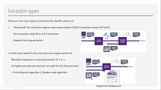
When capacitor is an inductor ... Part 1: Multidisciplinary product creation powered by your unconstrained network. Work concurrently across Challenges in scaling of interconnect delay. R, C delay in interconnects. Airgap for reducing the Thank you very much to Eric for very nice practical examples to show how important it is to think about currents flowing through ...

Photo Gallery

Parasitics in PCB Layout
How to Reduce Parasitic Capacitance in Your PCB Layout
How to Reduce Parasitic Capacitance in PCB Layout | Sierra Circuits
Flawless PCB design: RF rules of thumb - Part 1
Ground in PCB Layout - Separate or Not Separate? (with Rick Hartley)
EECE 2112 Module 53:  A Qualitative Viewpoint & Parasitic Circuit Elements
Parasitic Extraction and Back Annotation | VLSI Physical Design
PCB Layout Rules for Converters and Motor Drives
Flawless PCB design: 3 simple rules - Part 2
(Sponsored) PCB Traces 101 - Phil's Lab #112
Complete Multiphysics PCB Analysis with Altium and Ansys
EEVblog #1117 - PCB Power Plane Capacitance
View Detailed Profile
Parasitics in PCB Layout

Parasitics in PCB Layout

How do you simulate

How to Reduce Parasitic Capacitance in Your PCB Layout

How to Reduce Parasitic Capacitance in Your PCB Layout

Tech Consultant Zach Peterson continues exploring

How to Reduce Parasitic Capacitance in PCB Layout | Sierra Circuits

How to Reduce Parasitic Capacitance in PCB Layout | Sierra Circuits

PCB

Flawless PCB design: RF rules of thumb - Part 1

Flawless PCB design: RF rules of thumb - Part 1

Full course info: https://www.hans-rosenberg.com/epdc_information_yt?utm_source=yt-d-v1 Free mini-course: ...

Ground in PCB Layout - Separate or Not Separate? (with Rick Hartley)

Ground in PCB Layout - Separate or Not Separate? (with Rick Hartley)

Do you separate Digital GND and Analogue GND, or not? What do you think is better? Links: - Rick Hartley: ...

EECE 2112 Module 53:  A Qualitative Viewpoint & Parasitic Circuit Elements

EECE 2112 Module 53: A Qualitative Viewpoint & Parasitic Circuit Elements

This is a series of lectures from the Circuits I class taught at Vanderbilt University.

Parasitic Extraction and Back Annotation | VLSI Physical Design

Parasitic Extraction and Back Annotation | VLSI Physical Design

In this video concepts of

PCB Layout Rules for Converters and Motor Drives

PCB Layout Rules for Converters and Motor Drives

In this webinar, we will cover essential guidelines to ensure your GaN-based designs succeed from the start. In this webinar we ...

Flawless PCB design: 3 simple rules - Part 2

Flawless PCB design: 3 simple rules - Part 2

Full course info: https://www.hans-rosenberg.com/epdc_information_yt?utm_source=yt-d-v2 Free mini-course: ...

(Sponsored) PCB Traces 101 - Phil's Lab #112

(Sponsored) PCB Traces 101 - Phil's Lab #112

... Controlled impedance: https://www.protoexpress.com/blog/controlled-impedance-really-matters/

Complete Multiphysics PCB Analysis with Altium and Ansys

Complete Multiphysics PCB Analysis with Altium and Ansys

Follow Zachariah Peterson on LinkedIn: https://www.linkedin.com/in/zachariah-peterson/ Looking for

EEVblog #1117 - PCB Power Plane Capacitance

EEVblog #1117 - PCB Power Plane Capacitance

Are power planes in a 4 layer

Trace parasitic effects

Trace parasitic effects

Download and install PSpice® for TI https://www.ti.com/tool/PSPICE-FOR-TI This is the first video in the TI Precision Labs – Op ...

How to Reduce Noise in PCB Design

How to Reduce Noise in PCB Design

...

PCB Layout & Decoupling - Understanding Impedance (Part 2)

PCB Layout & Decoupling - Understanding Impedance (Part 2)

When capacitor is an inductor ... Part 1:

Should You Put an Inductor Above Ground? | PCB Layout

Should You Put an Inductor Above Ground? | PCB Layout

Multidisciplinary product creation powered by your unconstrained network. Work concurrently across

Modeling PCB Parasitics for Analog / Mixed-Signal Simulation

Modeling PCB Parasitics for Analog / Mixed-Signal Simulation

HyperLynx VX.2.6.

Parasitics in interconnects and Airgaps

Parasitics in interconnects and Airgaps

Challenges in scaling of interconnect delay. R, C delay in interconnects. Airgap for reducing the

PCB Layout Design and Component Values Adjustment for Matching Network Parasitics

PCB Layout Design and Component Values Adjustment for Matching Network Parasitics

Exploring

Watch How a PCB Layout Change Makes Big Difference - with Eric Bogatin (Ground bounce)

Watch How a PCB Layout Change Makes Big Difference - with Eric Bogatin (Ground bounce)

Thank you very much to Eric for very nice practical examples to show how important it is to think about currents flowing through ...