Media Summary: University of Hartford Saeid Moslehpour, by Geoff Miles. This video will provide an overview of IPC standards and the PCB Explore the process of making a custom PCB
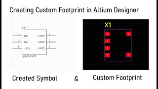
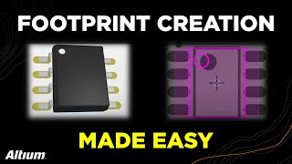
Padstack And Footprint Creation - Detailed Analysis & Overview
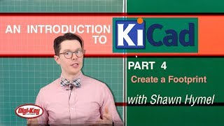
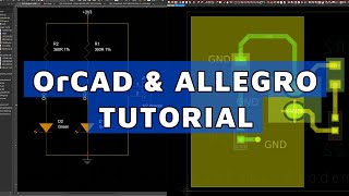
University of Hartford Saeid Moslehpour, by Geoff Miles. This video will provide an overview of IPC standards and the PCB Explore the process of making a custom PCB Learn about the user interface and GUI of the On part four of an introduction to KiCad V4.07, Shawn shows us how to create our own custom PCB Design Tutorial_25 Orcad Pcb Editor Custom Part 01 Footprint Creation
This video is an add on to "How to Import PCB