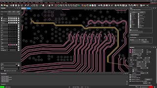
Media Summary: Optimizing your design shouldn't be a post-process. It should be considered as soon as you start La sbrogliatura dura circa 5 minuti con un pc di medie prestazioni. Electrons don't just travel from just pin to pin on single layers. They can travel in the z-axis through vias and pins as well as inside ...

Orcad Pcb Auto Routing - Detailed Analysis & Overview

Optimizing your design shouldn't be a post-process. It should be considered as soon as you start La sbrogliatura dura circa 5 minuti con un pc di medie prestazioni. Electrons don't just travel from just pin to pin on single layers. They can travel in the z-axis through vias and pins as well as inside ... Multidisciplinary product creation powered by your unconstrained network. Work concurrently across design, sourcing, and ... This video is part of the EasyEDA Quick Tips, where we share step-by-step I come up with this a long time ago and keep using it all the time. Links: - To learn how to design boards have a look at FEDEVEL ...

凱榮科技股份有限公司KairosTech Innovation Corp. T : +886-3-2753685 E : sales.com.tw ... PCB Design Tutorial_46 Orcad Pcb Editor Routing And Adding Vias 01 This demo quickly goes through some of the different

Photo Gallery

Cadence PCB Route Automatic 6 Signal Layers No Pin Limits
OrCAD X How To Series - Part 8 - First Pass Routing
Route Analysis | OrCAD PCB Designer
Using Auto Connect When Routing | Allegro PCB Designer
Orcad PCB auto routing
High-Speed Signal Routing : Z-Axis and Package Pin Delay | OrCAD PCB Designer
When to Use an Autorouter in PCB Design
Constraint Driven Routing | OrCAD PCB Designer
Quick Tips [PCB 12]: Auto routing Function
Cadence PCB Move With Autoroute
autorouting solution
Useful TIP: What Track Width To Use When Routing PCB?
View Detailed Profile
Cadence PCB Route Automatic 6 Signal Layers No Pin Limits

Cadence PCB Route Automatic 6 Signal Layers No Pin Limits

Here we explore

OrCAD X How To Series - Part 8 - First Pass Routing

OrCAD X How To Series - Part 8 - First Pass Routing

Ever wanted to lean How to create a

Route Analysis | OrCAD PCB Designer

Route Analysis | OrCAD PCB Designer

Optimizing your design shouldn't be a post-process. It should be considered as soon as you start

Using Auto Connect When Routing | Allegro PCB Designer

Using Auto Connect When Routing | Allegro PCB Designer

With

Orcad PCB auto routing

Orcad PCB auto routing

La sbrogliatura dura circa 5 minuti con un pc di medie prestazioni.

High-Speed Signal Routing : Z-Axis and Package Pin Delay | OrCAD PCB Designer

High-Speed Signal Routing : Z-Axis and Package Pin Delay | OrCAD PCB Designer

Electrons don't just travel from just pin to pin on single layers. They can travel in the z-axis through vias and pins as well as inside ...

When to Use an Autorouter in PCB Design

When to Use an Autorouter in PCB Design

Multidisciplinary product creation powered by your unconstrained network. Work concurrently across design, sourcing, and ...

Constraint Driven Routing | OrCAD PCB Designer

Constraint Driven Routing | OrCAD PCB Designer

A constraint driven approach makes your

Quick Tips [PCB 12]: Auto routing Function

Quick Tips [PCB 12]: Auto routing Function

This video is part of the EasyEDA Quick Tips, where we share step-by-step

Cadence PCB Move With Autoroute

Cadence PCB Move With Autoroute

Here we explore the

autorouting solution

autorouting solution

Autorouting

Useful TIP: What Track Width To Use When Routing PCB?

Useful TIP: What Track Width To Use When Routing PCB?

I come up with this a long time ago and keep using it all the time. Links: - To learn how to design boards have a look at FEDEVEL ...

How to Route Your PCB in OrCAD PCB Editor 17.4

How to Route Your PCB in OrCAD PCB Editor 17.4

This

Allegro Auto Route Demo

Allegro Auto Route Demo

凱榮科技股份有限公司KairosTech Innovation Corp. T : +886-3-2753685 E : sales@kairostech.com.tw ...

OrCAD X Presto - Duplicate or Redundant Traces and Routing in PCB Design

OrCAD X Presto - Duplicate or Redundant Traces and Routing in PCB Design

In

OrCAD Allegro Interactive Routing How-To

OrCAD Allegro Interactive Routing How-To

www.

PCB Design Tutorial_46 Orcad Pcb Editor Routing And Adding Vias 01

PCB Design Tutorial_46 Orcad Pcb Editor Routing And Adding Vias 01

PCB Design Tutorial_46 Orcad Pcb Editor Routing And Adding Vias 01

Allegro PCB Designer Demo - Advanced Routing Technologies

Allegro PCB Designer Demo - Advanced Routing Technologies

This demo quickly goes through some of the different

Cadence PCB Curve Routing

Cadence PCB Curve Routing

Here we explore the