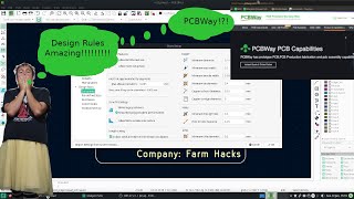
Media Summary: Thanks PCBWay for sponsoring this video - - Use this link for $5 new user free credit. In this video I'll ... This is a quick video demonstration on how to Seth Hillbrand explains some of the best loved and least known features of what you can do with

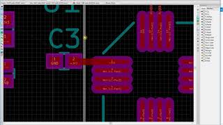
Kicad Lesson11 Pcb Design Rule Setting And Layout - Detailed Analysis & Overview

Thanks PCBWay for sponsoring this video - - Use this link for $5 new user free credit. In this video I'll ... This is a quick video demonstration on how to Seth Hillbrand explains some of the best loved and least known features of what you can do with In this short tutorial, I will show you how to For best development boards / components shop here : ** After creating the "COPPER FILL ZONE" with ...

Photo Gallery

KiCad Lesson11: pcb design rule setting and layout
How to Set Up Design Rules in KiCad | Sierra Circuits
KiCAD 7 PCB Layout in 5 steps
Boost Your KiCad Skills: 10 Essential PCB Layout Design Tips
Kicad Board Setup for JLCPCB
KiCad Tutorial for Beginners #10 - PCB Design Rule Checker, Drawing Rule Ares
Level up Your Custom Rules - KiCon Asia 2023
KiCad 6 STM32 PCB Design Full Tutorial - Phil's Lab #65
KiCad 6: Design Rules and Net Classes
PCB Design with KiCAD, part 5A: Setting Up The PCB's Design Rules
Setup Design Rules for PCB Kicad Tutorial 1.13C
KiCad Layout Vias and Board Modifications | Part 7 | PCB Design Tips
View Detailed Profile
KiCad Lesson11: pcb design rule setting and layout

KiCad Lesson11: pcb design rule setting and layout

www.micro-studios.com/lessons.

How to Set Up Design Rules in KiCad | Sierra Circuits

How to Set Up Design Rules in KiCad | Sierra Circuits

Before placing components in

KiCAD 7 PCB Layout in 5 steps

KiCAD 7 PCB Layout in 5 steps

In this video we will make a

Boost Your KiCad Skills: 10 Essential PCB Layout Design Tips

Boost Your KiCad Skills: 10 Essential PCB Layout Design Tips

Thanks PCBWay for sponsoring this video - https://pcbway.com/g/i8683S - Use this link for $5 new user free credit. In this video I'll ...

Kicad Board Setup for JLCPCB

Kicad Board Setup for JLCPCB

This is a quick video demonstration on how to

KiCad Tutorial for Beginners #10 - PCB Design Rule Checker, Drawing Rule Ares

KiCad Tutorial for Beginners #10 - PCB Design Rule Checker, Drawing Rule Ares

KiCad

Level up Your Custom Rules - KiCon Asia 2023

Level up Your Custom Rules - KiCon Asia 2023

Seth Hillbrand explains some of the best loved and least known features of what you can do with

KiCad 6 STM32 PCB Design Full Tutorial - Phil's Lab #65

KiCad 6 STM32 PCB Design Full Tutorial - Phil's Lab #65

Complete step-by-step

KiCad 6: Design Rules and Net Classes

KiCad 6: Design Rules and Net Classes

In this short tutorial, I will show you how to

PCB Design with KiCAD, part 5A: Setting Up The PCB's Design Rules

PCB Design with KiCAD, part 5A: Setting Up The PCB's Design Rules

In this edition of The Hive's "

Setup Design Rules for PCB Kicad Tutorial 1.13C

Setup Design Rules for PCB Kicad Tutorial 1.13C

Setup Design Rules

KiCad Layout Vias and Board Modifications | Part 7 | PCB Design Tips

KiCad Layout Vias and Board Modifications | Part 7 | PCB Design Tips

KiCad Layout

#10 How To Do PCB Routing In KiCad 7.0  with Basic PCB Design Rules | #PCBCupid

#10 How To Do PCB Routing In KiCad 7.0 with Basic PCB Design Rules | #PCBCupid

For best development boards / components shop here : https://shop.pcbcupid.com ** After creating the "COPPER FILL ZONE" with ...

KiCad Tutorial  - Setting up your clearance and track width rules for your PCB Design.

KiCad Tutorial - Setting up your clearance and track width rules for your PCB Design.

KiCad

6 Horribly Common PCB Design Mistakes

6 Horribly Common PCB Design Mistakes

Grab your free