Media Summary: Recognising the need for a robust and reliable sample preparation technique, The Bridge approached An important group of devices is formed by bonding PDMS to patterned glass substrates. The following short video shows how ... Dr. James McVittie goes into further detail on Dry
Henniker Plasma Plasma Etching Explained - Detailed Analysis & Overview
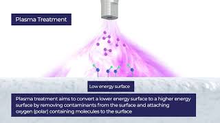
Recognising the need for a robust and reliable sample preparation technique, The Bridge approached An important group of devices is formed by bonding PDMS to patterned glass substrates. The following short video shows how ... Dr. James McVittie goes into further detail on Dry It seems that the weight of the world rests on high-technology, from robotics to smart phones. High technology is solely enabled by ...