Media Summary: After this tutorial you will know how to start designing your own boards in Cadence PCB Editor Timing Vision Tutorial This demo quickly goes through some of the different
Cadence Pcb Route Vision - Detailed Analysis & Overview
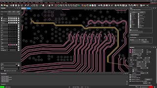
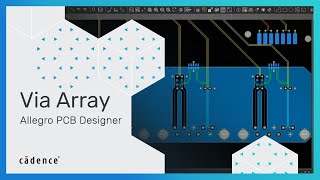
After this tutorial you will know how to start designing your own boards in Cadence PCB Editor Timing Vision Tutorial This demo quickly goes through some of the different Even the best engineers spend a bulk of time placing and Easily add vias arrays or via structures in various patterns to your designs. This way you can ensure proper EMC performance and ... With auto connect you can simply window select a set of nets and connect the pins of your components. Learn more about