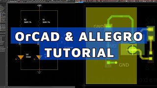
Media Summary: After this tutorial you will know how to start designing your own boards in Re-creating similar placement in multiple designs is probably not the most productive use of your time. With This Asset will guide you do a crossprobe between

Cadence Pcb Component Lead Editor - Detailed Analysis & Overview

After this tutorial you will know how to start designing your own boards in Re-creating similar placement in multiple designs is probably not the most productive use of your time. With This Asset will guide you do a crossprobe between In this series. Adam Fuchs, Product Engineer at This video will demonstrate how to cross probe, cross-select, and cross place between DESIGN ENTRY - HDL and Dr. Saeid Moslehpour University of Hartford Department of Electrical and Computer Engineering By Mike DiPanfilo & FerdinandĀ ...

This video will provide an overview of IPC standards and the

Photo Gallery

Cadence PCB Component Lead Editor
Tutorial OrCAD and Cadence Allegro PCB Editor | 2022 | Step by Step | For Beginners
Cadence OrCad PCB Editor 17.4 (Creating Custom Footprints)
Importing and exporting component placement | Allegro PCB Designer
How to Crossprobe and Place Components Between Allegro Design Entry CIS and PCB Editor
OrCAD X - How to Series - Part 3 - Cross Section Editing
Easy methods of component placement on your PCB | Allegro PCB Designer
Allegro PCB Designer Demo - Component Placement
The Allegro PCB Editor SKILL Form Interface
How to Crossprobe and Crossplace Components Between Design Entry HDL and Allegro PCB Editor
Cadence PCB Editor Syncing Components
Cadence OrCad PCB Editor 17.4 (Complete board layout in 30 min)
View Detailed Profile
Cadence PCB Component Lead Editor

Cadence PCB Component Lead Editor

Here we explore the

Tutorial OrCAD and Cadence Allegro PCB Editor | 2022 | Step by Step | For Beginners

Tutorial OrCAD and Cadence Allegro PCB Editor | 2022 | Step by Step | For Beginners

After this tutorial you will know how to start designing your own boards in

Cadence OrCad PCB Editor 17.4 (Creating Custom Footprints)

Cadence OrCad PCB Editor 17.4 (Creating Custom Footprints)

Explore the process of making a custom

Importing and exporting component placement | Allegro PCB Designer

Importing and exporting component placement | Allegro PCB Designer

Re-creating similar placement in multiple designs is probably not the most productive use of your time. With

How to Crossprobe and Place Components Between Allegro Design Entry CIS and PCB Editor

How to Crossprobe and Place Components Between Allegro Design Entry CIS and PCB Editor

This Asset will guide you do a crossprobe between

OrCAD X - How to Series - Part 3 - Cross Section Editing

OrCAD X - How to Series - Part 3 - Cross Section Editing

In this series. Adam Fuchs, Product Engineer at

Easy methods of component placement on your PCB | Allegro PCB Designer

Easy methods of component placement on your PCB | Allegro PCB Designer

Allegro PCB

Allegro PCB Designer Demo - Component Placement

Allegro PCB Designer Demo - Component Placement

This demo goes over some features within

The Allegro PCB Editor SKILL Form Interface

The Allegro PCB Editor SKILL Form Interface

The

How to Crossprobe and Crossplace Components Between Design Entry HDL and Allegro PCB Editor

How to Crossprobe and Crossplace Components Between Design Entry HDL and Allegro PCB Editor

This video will demonstrate how to cross probe, cross-select, and cross place between DESIGN ENTRY - HDL and

Cadence PCB Editor Syncing Components

Cadence PCB Editor Syncing Components

Dr. Saeid Moslehpour University of Hartford Department of Electrical and Computer Engineering By Mike DiPanfilo & FerdinandĀ ...

Cadence OrCad PCB Editor 17.4 (Complete board layout in 30 min)

Cadence OrCad PCB Editor 17.4 (Complete board layout in 30 min)

Complete

OrCAD X Quick Tips - Footprint Authoring

OrCAD X Quick Tips - Footprint Authoring

The

Tutorial Cadence Lead Editor

Tutorial Cadence Lead Editor

Here we explore the

Step by step Guide for Placing External Library Partner Components in the OrCAD X Capture Schematic

Step by step Guide for Placing External Library Partner Components in the OrCAD X Capture Schematic

OrCAD

How to Create IPC Compliant Footprint in OrCAD PCB Editor 17.4

How to Create IPC Compliant Footprint in OrCAD PCB Editor 17.4

This video will provide an overview of IPC standards and the