Media Summary: Multidisciplinary product creation powered by your unconstrained network. Work concurrently across design, sourcing, and ... In this video I will show 3 ways to set up and use the Freerouting Autorouter plugin for KiCAD For best development boards / components shop here : ** After creating the "COPPER FILL ZONE" with ...
7 Routing The Pcb - Detailed Analysis & Overview
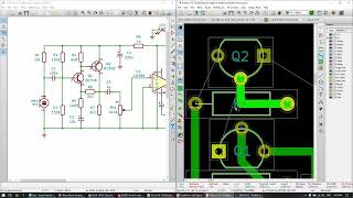
Multidisciplinary product creation powered by your unconstrained network. Work concurrently across design, sourcing, and ... In this video I will show 3 ways to set up and use the Freerouting Autorouter plugin for KiCAD For best development boards / components shop here : ** After creating the "COPPER FILL ZONE" with ... If you are interested, you can download this AD: This video includes a paid promotion for JLCPCB.) Some tips for when designing hardware and Just a quick little video. Become a Patreon supporter to help the channel continue to grow: ...
I come up with this a long time ago and keep using it all the time. Links: - To learn how to design boards have a look at FEDEVEL ... Thanks PCBWay for sponsoring this video - - Use this link for $5 new user free credit. In this video I'll ...