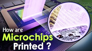
Media Summary: Interested in working on the forefront of technological innovation at ASML? Discover here: ... Try SendCutSend 15% off for your next project! My descent into madness, chasing one ... What does it take to print billions of transistors with nanometer precision? It's a joint effort, one that brings together both hardware ...

Photo Lithography Lithography - Detailed Analysis & Overview

Interested in working on the forefront of technological innovation at ASML? Discover here: ... Try SendCutSend 15% off for your next project! My descent into madness, chasing one ... What does it take to print billions of transistors with nanometer precision? It's a joint effort, one that brings together both hardware ... Bernd Geh The Key of Micro- and Nanoelectronics: Basics of In this video I demonstrate how I used a Carl Zeiss S-planar wafer stepper lens to do micron-size Over the years, semiconductors have drastically shrunk in size. Computers used to take up entire rooms, and now we have ...

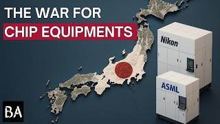
Japan's Nikon and the Dutch company ASML had once vied for dominance in the crucial Though the name sounds a bit intimidating, Bringing Moore's Law to the garage with a DLP maskless British Instructional Films Ltd presents a Classroom Film. A small child turns the pages of a book. He looks closely at the ... In this process, eight steps are involved: wafer manufacturing, oxidation, Join Art Gallery of St. Albert as we get an inside look at the

Like a camera that captures scenes on film with light,

Photo Gallery

Photolithography: Step by step
The $200M Machine that Prints Microchips:  The EUV Photolithography System
Speedrunning 30yrs of lithography technology
Computational lithography: Driving nanometer precision in microchip manufacturing | ASML
Photolithography Overview for MEMS
How Photolithography works | Part 1/6 – Introduction
DIY Semiconductor Patterning
How Photolithography works | Part 4/6 – Imaging Process
DIY Photolithography using 1980s Carl Zeiss S-Planar Lens (405nm)
How to make a lithographic print | National Museums Liverpool
How EUV lithography works
The Lithography Wars: The Story of How Nikon Lost to ASML
View Detailed Profile
Photolithography: Step by step

Photolithography: Step by step

Photolithography: Step by step

The $200M Machine that Prints Microchips:  The EUV Photolithography System

The $200M Machine that Prints Microchips: The EUV Photolithography System

Interested in working on the forefront of technological innovation at ASML? Discover here: ...

Speedrunning 30yrs of lithography technology

Speedrunning 30yrs of lithography technology

Try SendCutSend 15% off for your next project! https://sendcutsend.com/breakingtaps/ My descent into madness, chasing one ...

Computational lithography: Driving nanometer precision in microchip manufacturing | ASML

Computational lithography: Driving nanometer precision in microchip manufacturing | ASML

What does it take to print billions of transistors with nanometer precision? It's a joint effort, one that brings together both hardware ...

Photolithography Overview for MEMS

Photolithography Overview for MEMS

This is a short overview of the

How Photolithography works | Part 1/6 – Introduction

How Photolithography works | Part 1/6 – Introduction

Bernd Geh | The Key of Micro- and Nanoelectronics: Basics of

DIY Semiconductor Patterning

DIY Semiconductor Patterning

DIY

How Photolithography works | Part 4/6 – Imaging Process

How Photolithography works | Part 4/6 – Imaging Process

Bernd Geh | The Key of Micro- and Nanoelectronics: Basics of

DIY Photolithography using 1980s Carl Zeiss S-Planar Lens (405nm)

DIY Photolithography using 1980s Carl Zeiss S-Planar Lens (405nm)

In this video I demonstrate how I used a Carl Zeiss S-planar wafer stepper lens to do micron-size

How to make a lithographic print | National Museums Liverpool

How to make a lithographic print | National Museums Liverpool

Lithography

How EUV lithography works

How EUV lithography works

Over the years, semiconductors have drastically shrunk in size. Computers used to take up entire rooms, and now we have ...

The Lithography Wars: The Story of How Nikon Lost to ASML

The Lithography Wars: The Story of How Nikon Lost to ASML

Japan's Nikon and the Dutch company ASML had once vied for dominance in the crucial

Photo Lithography on Clay: A Surprisingly Simple Way to Print Images On Clay - KRISTINA BOGDANOV

Photo Lithography on Clay: A Surprisingly Simple Way to Print Images On Clay - KRISTINA BOGDANOV

Though the name sounds a bit intimidating,

Electron Beam Lithography

Electron Beam Lithography

How does E-beam

Maskless Photolithography Stepper for Homemade Chips

Maskless Photolithography Stepper for Homemade Chips

Bringing Moore's Law to the garage with a DLP maskless

Lithography (1940-1949)

Lithography (1940-1949)

British Instructional Films Ltd presents a Classroom Film. A small child turns the pages of a book. He looks closely at the ...

‘Semiconductor Manufacturing Process’ Explained | 'All About Semiconductor' by Samsung Semiconductor

‘Semiconductor Manufacturing Process’ Explained | 'All About Semiconductor' by Samsung Semiconductor

In this process, eight steps are involved: wafer manufacturing, oxidation,

Photo Lithography with Amanda McKenzie

Photo Lithography with Amanda McKenzie

Join Art Gallery of St. Albert as we get an inside look at the

How Photolithography works | Part 2/6 – Photolithography Basics

How Photolithography works | Part 2/6 – Photolithography Basics

Bernd Geh | The Key of Micro- and Nanoelectronics: Basics of

Samsung Semiconductor Explains Photo Lithography and EUV in 5 Minutes

Samsung Semiconductor Explains Photo Lithography and EUV in 5 Minutes

Like a camera that captures scenes on film with light,